
- English
- Español
- Português
- русский
- Français
- 日本語
- Deutsch
- tiếng Việt
- Italiano
- Nederlands
- ภาษาไทย
- Polski
- 한국어
- Svenska
- magyar
- Malay
- বাংলা ভাষার
- Dansk
- Suomi
- हिन्दी
- Pilipino
- Türkçe
- Gaeilge
- العربية
- Indonesia
- Norsk
- تمل
- český
- ελληνικά
- український
- Javanese
- فارسی
- தமிழ்
- తెలుగు
- नेपाली
- Burmese
- български
- ລາວ
- Latine
- Қазақша
- Euskal
- Azərbaycan
- Slovenský jazyk
- Македонски
- Lietuvos
- Eesti Keel
- Română
- Slovenski
- मराठी
- Srpski језик


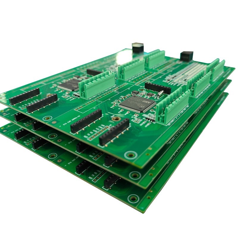
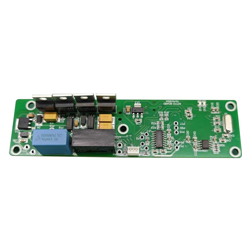
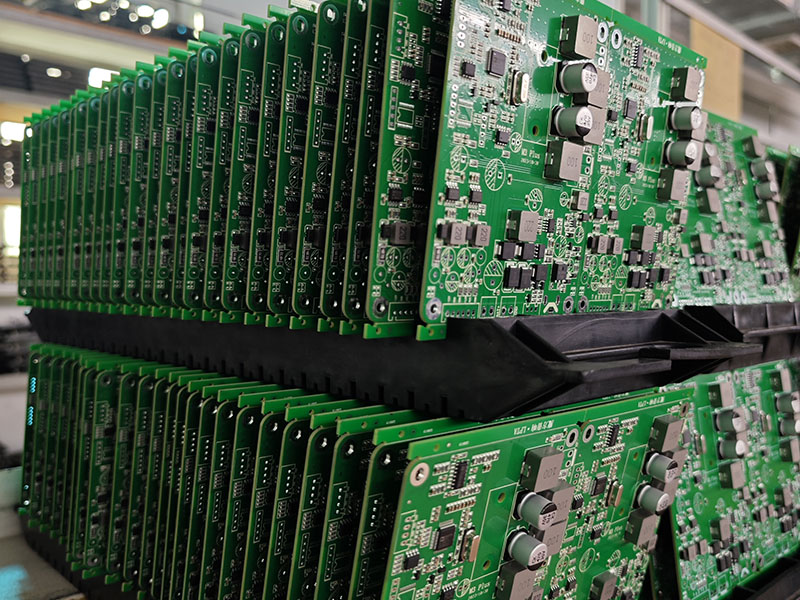
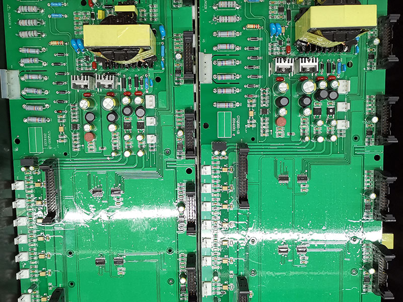
Paper Shredder PCBA
Unixplore Electronics is a Chinese company that has been focusing on creating and producing first-class Paper Shredder PCBA since 2008. We have certifications to ISO9001:2015 and IPC-610E PCB assembly standards.
Model:UE-205
Send Inquiry
Product Description
How to select electronic components for a Paper Shredder PCBA?
Unixplore Electronics has been committed to the development and manufacturing of high-quality Paper Shredder PCBA in the form of OEM and ODM type since 2011.
When selecting electronic components for a Paper Shredder PCBA, the following points should be considered:
Functional Requirements: First, determine the functions the paper shredder PCBA needs to perform, including start, stop, reverse, and overload protection. Then, select appropriate components based on these functional requirements.
Performance Requirements: Based on the design performance specifications, such as operating voltage, current, frequency, and accuracy, select components that meet the requirements to ensure stable and reliable operation.
Reliability: Consider the reliability and lifespan of components during selection. Choose reputable suppliers and brands to ensure product stability and durability.
Cost-Effectiveness: While ensuring performance, consider the cost of components and select components with a high cost-performance ratio to make the product competitive.
Package Type: Select the appropriate package type based on the PCB layout and size limitations to ensure that components can be correctly mounted on the PCB and maintain good heat dissipation.
Supply Stability: Select components with a stable supply to ensure long-term supply support and avoid production delays caused by component shortages or production stoppages.
Compatibility: Ensure the selected components are compatible with other components and control boards to avoid instability or conflicts caused by compatibility issues.
Taking all the above factors into account, carefully select each component to ensure they are properly matched to meet design requirements and ultimately guarantee the stable performance and reliability of the paper shredder PCBA.
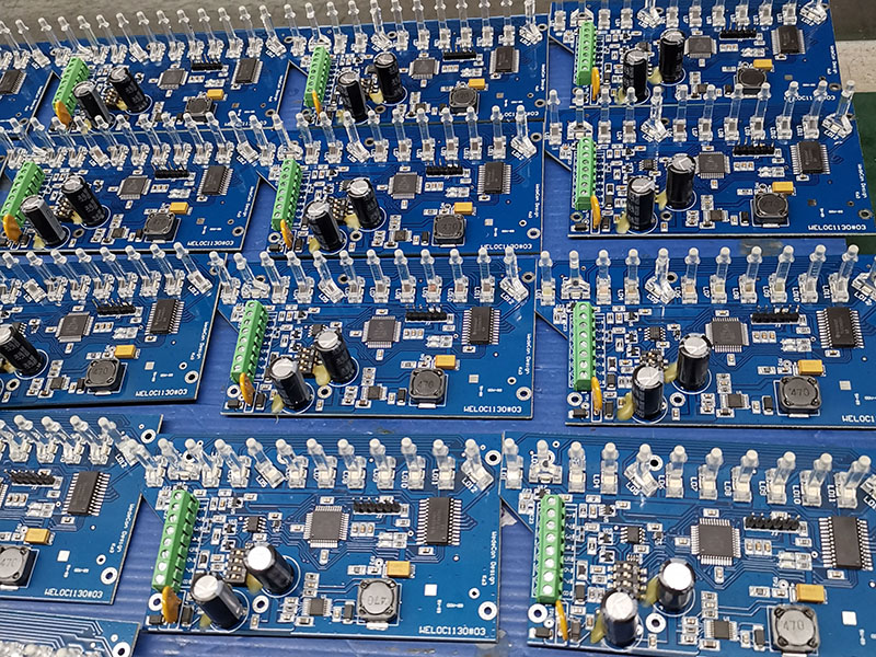
Paper Shredder PCBA Manufacture
* Gerber file and BOM list supplied by client
* Bare PCB produced, components purchased by us
* PCB fabrication with parts fully assembled
* 100% Functionally Tested OK prior to shipping
* RoHS compliant, Lead-free manufacturing process
* Quick delivery, with independent ESD package
* One stop electronic manufacturing service for PCB design, PCB layout, PCB manufacture, components procurement, PCB SMT and DIP assembly, IC programming, function test, packaging and delivery
Unixplore PCB & PCB Assembly Capability
| Parameter | Capability |
| Layers | 1-40 layers |
| Assembly Type | Through-Hole (THT), Surface Mount (SMT), Mixed (THT+SMT) |
| Minimum Component Size | 0201(01005 Metric) |
| Maximum Component Size | 2.0 in x 2.0 in x 0.4 in (50 mm x 50 mm x 10 mm) |
| Component Package Types | BGA, FBGA, QFN, QFP, VQFN, SOIC, SOP, SSOP, TSSOP, PLCC, DIP, SIP, etc. |
| Minimum Pad Pitch | 0.5 mm (20 mil) for QFP, QFN, 0.8 mm (32 mil) for BGA |
| Minimum Trace Width | 0.10 mm (4 mil) |
| Minimum Trace Clearance | 0.10 mm (4 mil) |
| Minimum Drill Size | 0.15 mm (6 mil) |
| Maximum Board Size | 18 in x 24 in (457 mm x 610 mm) |
| Board Thickness | 0.0078 in (0.2 mm) to 0.236 in (6 mm) |
| Board Material | CEM-3,FR-2,FR-4, High-Tg, HDI, Aluminum, High Frequency, FPC, Rigid-Flex, Rogers, etc. |
| Surface Finish | OSP, HASL, Flash Gold, ENIG, Gold Finger, etc. |
| Solder Paste Type | Leaded or Lead-Free |
| Copper Thickness | 0.5OZ – 5 OZ |
| Assembly Process | Reflow Soldering, Wave Soldering, Manual Soldering |
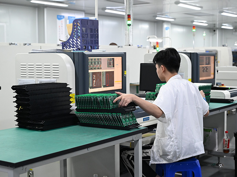
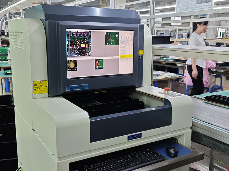
| Inspection Methods | Automated Optical Inspection (AOI), X-ray, Visual Inspection |
| Testing Methods In-House | Functional Test, Probe Test, Aging Test, High and Low Temperature Test |
| Turnaround Time | Sampling: 24 hours to 7 days, Mass Run: 10 - 30 days |
| PCB Assembly Standards | ISO9001:2015; ROHS, UL 94V0, IPC-610E class ll |
Unixplore Value-Added EMS Service
● IC pre-programming service with file in format of HEX,ELF and BIN.
● Paper Shredder PCBA Function test fixture customized according to client’s test requirements
● Box building service including plastic & metal case mold and part production
● Conformal coating including selective lacquer coating, epoxy resin potting
● Wire harness and cable assembly
● Finished product assembly including box, screen, membrane switch, labelling and customized carton or retail box packing.
● Various third-party tests for PCBA are available upon request
● Product Certification Assistance
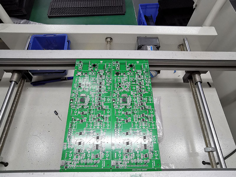
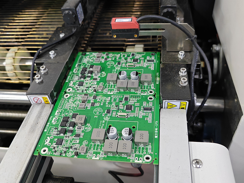
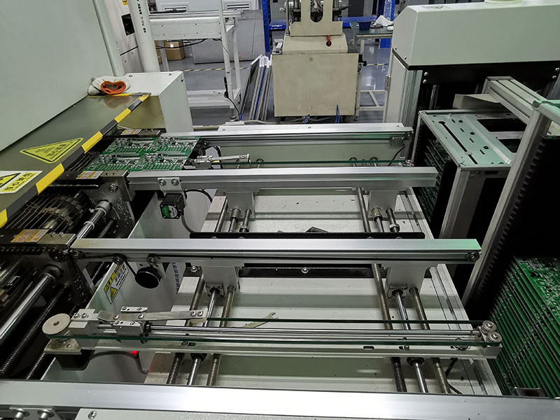
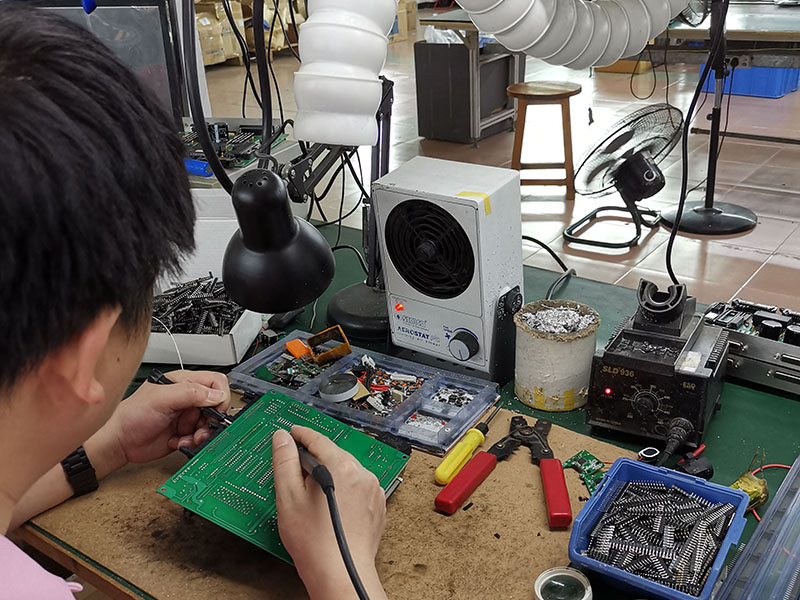
PCBA Production Procedure
-
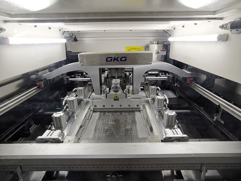
1. Automatic solderpaste printing
-
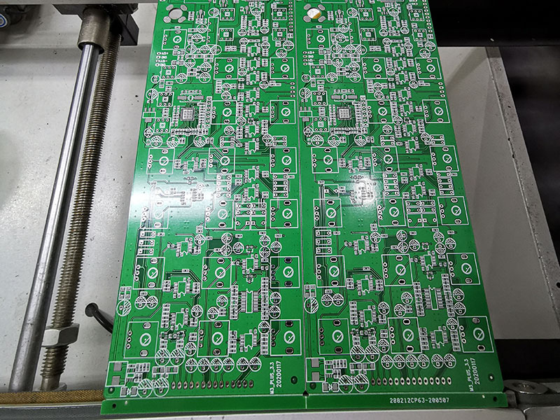
2. solderpaste printing done
-
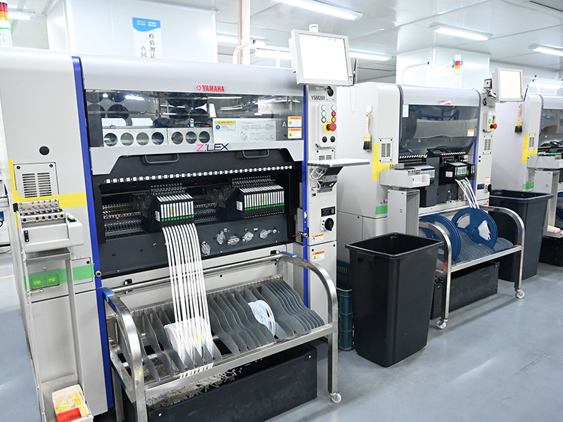
3. SMT pick and place
-
4. SMT pick and place done
-
5. ready for reflow soldering
-
6. reflow soldering done
-
7. ready for AOI
-
8. AOI inspection process
-
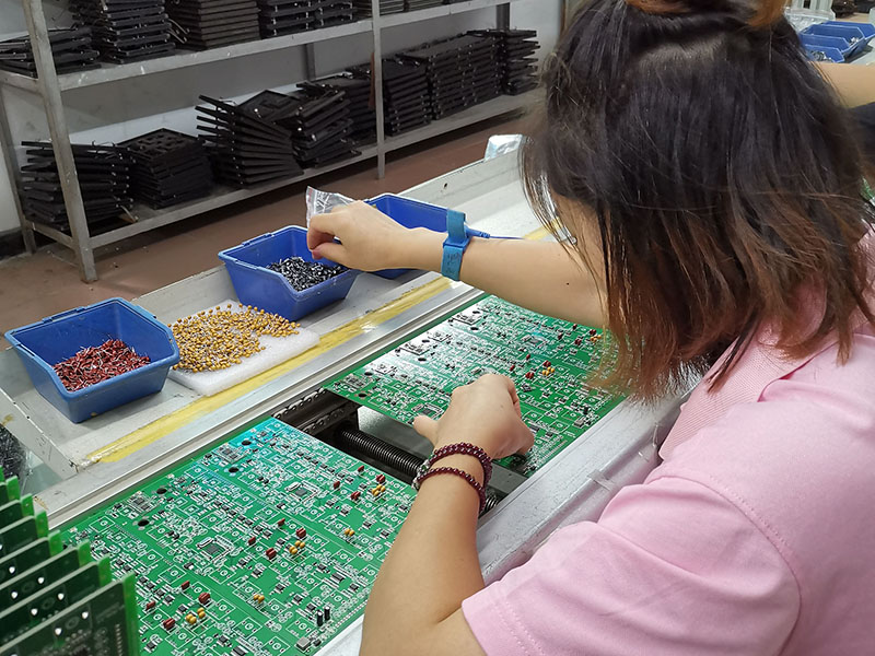
9. THT component placement
-
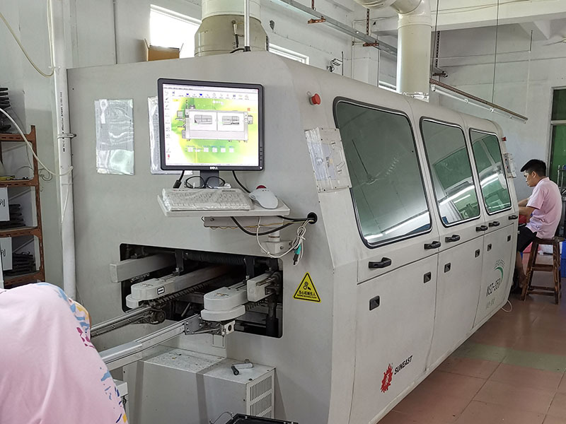
10. wave soldering process
-
11. THT assembly done
-
12. AOI Inspection for THT assembly
-
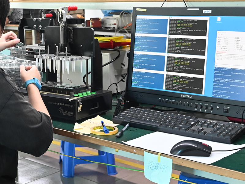
13. IC programming
-
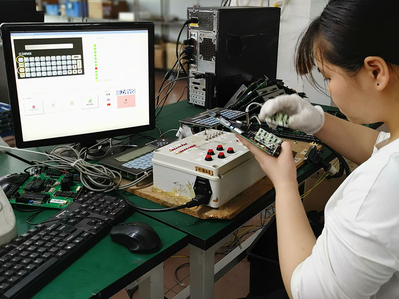
14. function test
-
15. QC Check and Repair
-
16. PCBA conformal coating Process
-
17. ESD packing
-
18. Ready for Shipping
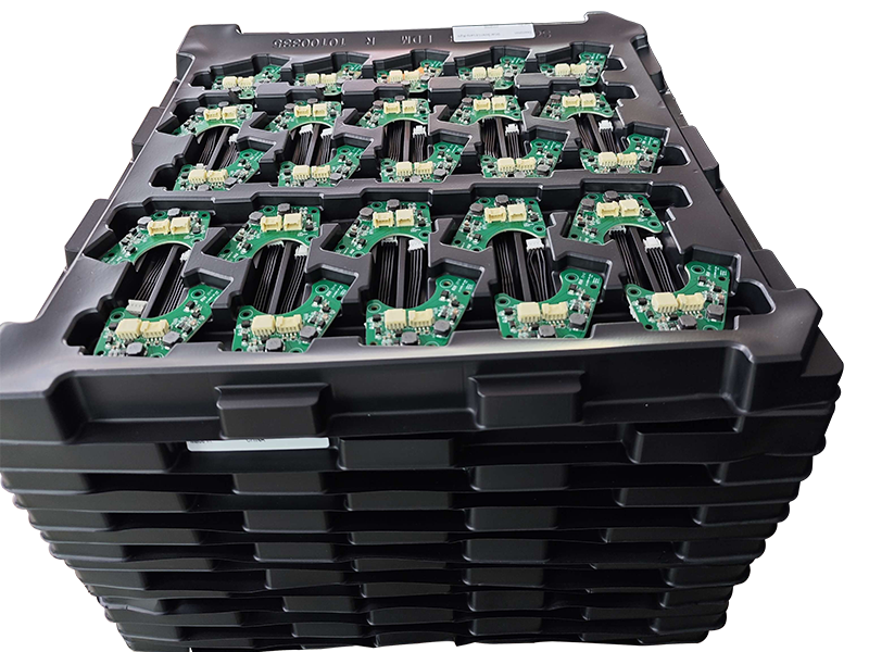
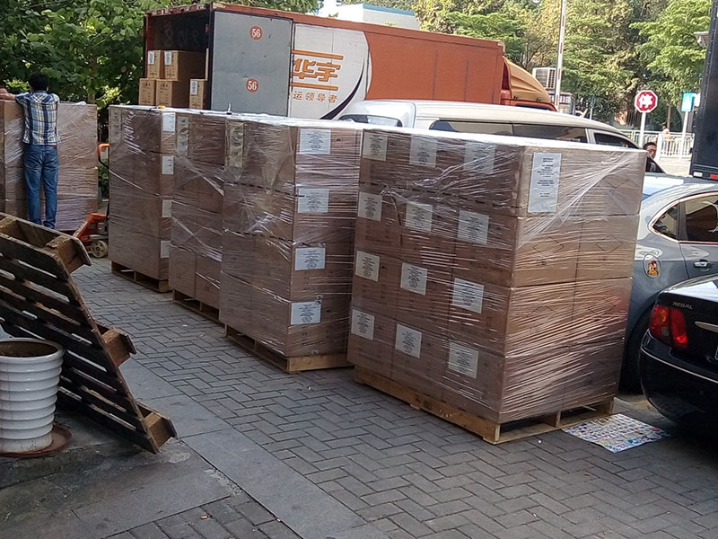
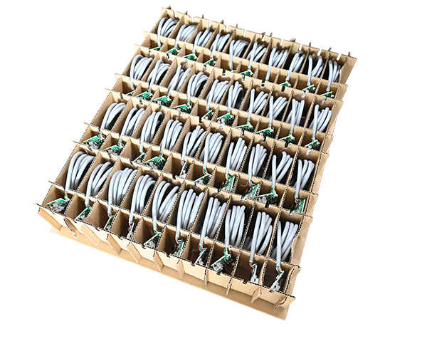
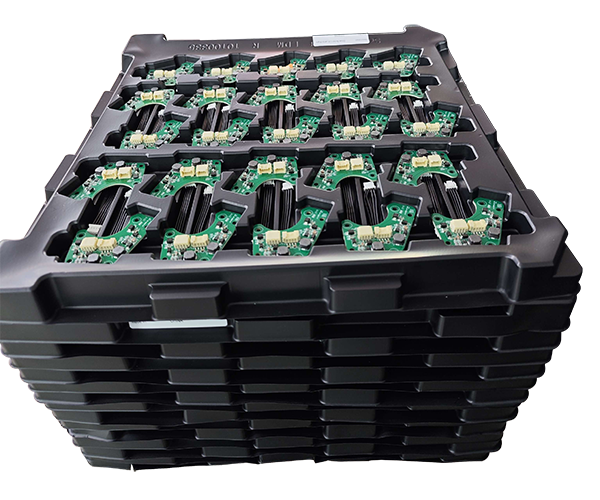
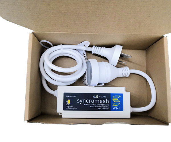
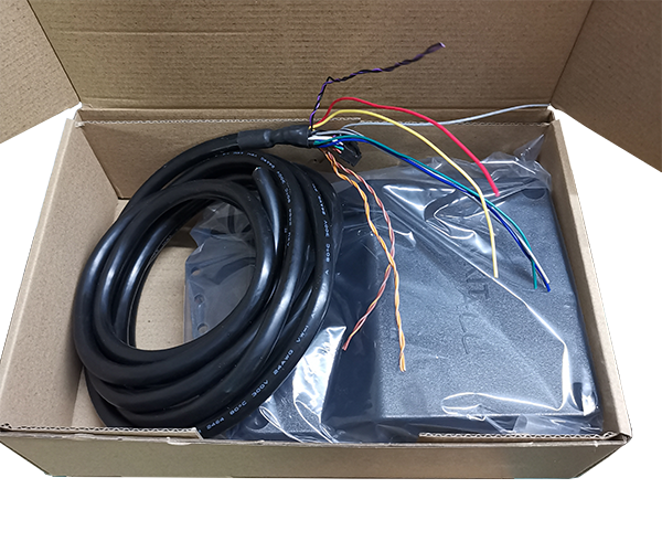
Packaging
For PCBA
For Finished Product
Hot Tags: Paper Shredder PCBA, China, Manufacturers, Suppliers, Factory, Customized, Cheap, Quality, Advanced, CE, 1 Year Warranty, Price
Product Tag
Related Category
Home Appliance PCBA
Industrial Control PCBA
Automobile PCBA
Consumer Electronics PCBA
Medical Equipment PCBA
Security System PCBA
Healthcare PCBA
LED Lighting PCBA
IoT PCBA
Electric Gardening Tool PCBA
Send Inquiry
Please Feel free to give your inquiry in the form below. We will reply you in 24 hours.


