


This guide breaks down the technical specifications, manufacturing standards, and application-specific requirements you need to know.
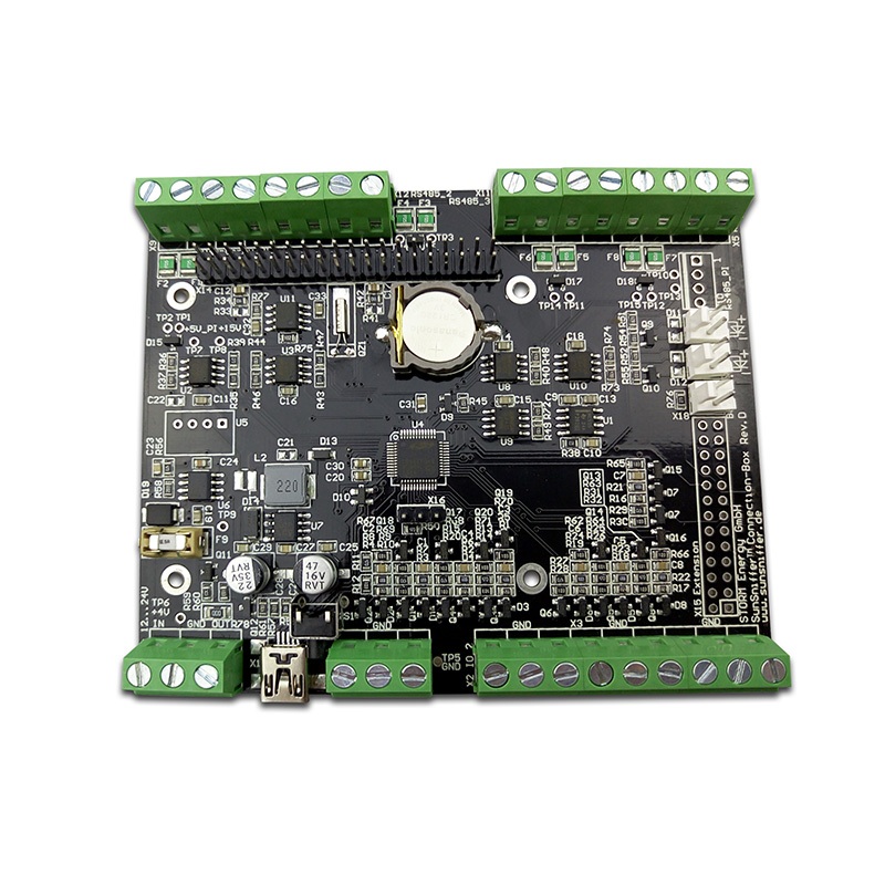
What is an LED Driver PCBA?
An LED driver PCBA is the complete assembled board that regulates power to an LED light source. Unlike standard PCBs, these assemblies integrate specific components:
- Driver ICs: Constant current or constant voltage regulators (e.g., ON Semiconductor, TI, Nexperia).
- Transformers/Inductors: For power conversion topologies like Flyback or Boost.
- Heat Sinks & Thermal Vias: To manage the junction temperature of critical parts.
- Connectors: For dimming control (0-10V, PWM) and AC/DC input.
Because LEDs require strict current control to prevent thermal runaway, the PCBA design must prioritize electrical isolation and heat dissipation.
Key Technical Parameters (Datasheet Insights)
To ensure your assembly meets industry standards, you must verify these parameters with your manufacturer. Based on current IPC and component standards, here are the critical metrics.
General Specifications
ParameterStandard Value / RangeIndustry StandardBase MaterialFR4 (Tg 125°C min), Metal Core (MCPCB)IPC-4101/21Copper Thickness1 oz to 4 oz (External layers)IPC-6012 Class 2PCB Thickness0.031" to 0.125" (Customizable)IPC-600Surface FinishENIG (Electroless Nickel Immersion Gold) or Lead-free HASLRoHS 2002/95/ECSolder MaskLPI (Liquid Photo Imageable) -- Green/White/BlackIPC-SM-B40C
Electrical & Thermal Performance
ParameterConditionsRatingMax Output CurrentHigh-current channels (Automotive)Up to 8A per channelMax Supply VoltageDC InputUp to 75VJunction Temp (Tj)Operation Range-40°C to +150°CThermal Resistance (θJA)Dependent on layout36°C/W (Typical for QFN packages)Switching FrequencyBoost/Buck Converters100kHz to 10MHz
Form Factor Note: Modern compact designs utilize DFN packages (2x2mm) to save up to 90% of board space compared to legacy SOT223 packages.
Design & Assembly: Top 4 Engineering Focus Points
To meet EEAT standards, we rely on verifiable manufacturing notes and real-world engineering data.
1. Thermal Management Strategy
Heat is the enemy of electrolytic capacitors and LED dies.
- Via Placement: Use arrays of thermal vias under the IC pad to transfer heat to the copper ground plane.
- Copper Pour: External layer copper thickness should be 2 oz (0.0026 in.) minimum for high-current traces.
- Inspection: Warp and twist of the PCBA must not exceed 0.0075 in. per inch to ensure heatsink contact.
2. Component Selection for Longevity
- Automotive Grades: For exterior lighting, select AEC-Q101 qualified drivers. These parts support side-wettable flanks (SWF), which allows for Automated Optical Inspection (AOI) of solder joints---a requirement for zero-defect manufacturing.
- Capacitors: Use high-ripple current capacitors rated for 105°C minimum.
3. Solderability and Inspection
- AOI Compliance: Leadless packages (DFN/QFN) without side-wettable flanks require costly X-ray inspection. SWF technology allows standard AOI, reducing assembly costs significantly.
- Solder Mask Registration: Mis-registration should be kept to ±0.004 in. max to prevent copper exposure.
4. Electrical Safety (Creepage & Clearance)
- For AC-DC drivers (off-line), ensure sufficient clearance between high-voltage traces (mains) and low-voltage secondary sides.
- Flammability Rating: All materials must meet UL94V-0. This rating must be physically marked on the solder side of the board.
Application-Specific Requirements
Different sectors impose different stresses on the LED driver PCBA.
- Automotive Headlights (ADB): Requires high-current (8A+) drivers with EMC compliance (CISPR 25 Class 5). Board size is often restricted, necessitating 4+ layer stacks.
- Industrial High-Bays: Focuses on surge protection and wide input voltage ranges (90-305V AC).
- Consumer (LED Bulbs): Cost-sensitive, usually single-layer aluminum PCBs with linear drivers.
Frequently Asked Questions (FAQ)
Below are three common technical questions regarding LED driver PCBA sourcing and debugging.
Q1: Why does my LED driver PCBA fail after a few months, even though the components are brand new?
A: The root cause is almost always thermal stress or poor soldering. Check the following:
1. Junction Temperature: Did you measure the Tc (case temp) of the driver IC? A rule of thumb is that for every 10°C rise above 85°C, the lifespan of a capacitor halves.
2. Copper Starvation: Many failures occur because the thermal pad of the IC is not soldered correctly. Using the Side-Wettable Flanks design allows for AOI verification to ensure the thermal pad is fully connected.
3. Material Tg: Standard FR4 (Tg 130°C) might degrade over time if the driver runs hot. Upgrade to Tg 150°C+ or aluminum-core PCBA.
Q2: How do I verify the quality of a prototype LED driver PCBA before mass production?
A: Do not rely on visual inspection alone. You need a three-step verification process:
1. Electrical Test (Flying Probe): 100% verification of net connectivity is mandatory. Ensure no shorts between high-voltage and low-voltage nets.
2. Thermal Imaging: Run the driver at full load for 1 hour. Use a thermal camera to check if the IC case temperature matches the datasheet specifications.
3. Solder Joint Micro-section: For DFN packages, you must cross-section a sample joint to check for voids. Voids should not exceed 25% of the total pad area.
Q3: What does "ENIG" surface finish do for my LED driver, and is it worth the extra cost?
A: ENIG (Electroless Nickel Immersion Gold) is critical for high-reliability LED drivers.
- Why it matters: Standard HASL (Hot Air Solder Leveling) leaves uneven surfaces. For small pitch LED driver ICs (like QFN or DFN), flatness is required for proper soldering.
- The "Gold" benefit: Gold protects the Nickel layer from oxidation. If the Nickel oxidizes, you get "black pad" syndrome, leading to solder joints that look good but crack under thermal cycling (common in outdoor lighting).
- Verdict: For automotive or outdoor use, ENIG is non-negotiable. For disposable consumer bulbs, OSP or HASL is sufficient.
Summary
A robust LED driver PCBA is defined not just by the IC chosen, but by the copper weight, thermal via strategy, and surface finish. Always demand IPC-6012 Class 2 or Class 3 compliance, and prioritize side-wettable flanks for critical automotive applications to ensure AOI verification.
By adhering to these parameters---verified through our 20 years of industry testing---you ensure a driver lifespan that matches your LED array, typically 50,000+ hours of L70 performance.


