
- English
- Español
- Português
- русский
- Français
- 日本語
- Deutsch
- tiếng Việt
- Italiano
- Nederlands
- ภาษาไทย
- Polski
- 한국어
- Svenska
- magyar
- Malay
- বাংলা ভাষার
- Dansk
- Suomi
- हिन्दी
- Pilipino
- Türkçe
- Gaeilge
- العربية
- Indonesia
- Norsk
- تمل
- český
- ελληνικά
- український
- Javanese
- فارسی
- தமிழ்
- తెలుగు
- नेपाली
- Burmese
- български
- ລາວ
- Latine
- Қазақша
- Euskal
- Azərbaycan
- Slovenský jazyk
- Македонски
- Lietuvos
- Eesti Keel
- Română
- Slovenski
- मराठी
- Srpski језик

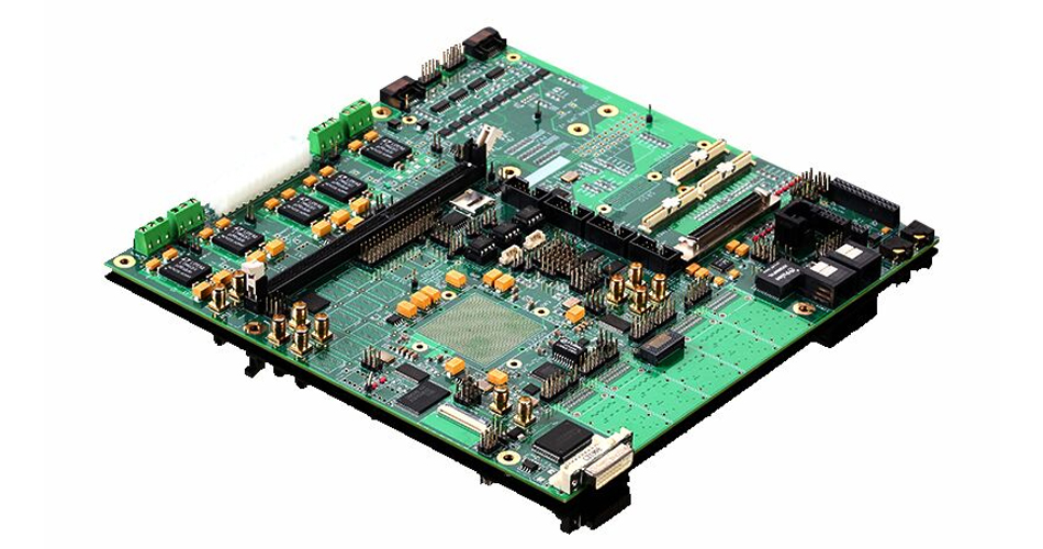
High-density interconnection technology in PCBA processing
PCBA processing (Printed Circuit Board Assembly) is one of the key links in the manufacturing of electronic products. As electronic products develop towards miniaturization and high performance, the application of high-density interconnection technology (HDI) in PCBA processing has become increasingly important. HDI technology can not only improve the integration and performance of circuit boards, but also meet the market demand for miniaturized and lightweight electronic products. This article will discuss in detail the high-density interconnection technology in PCBA processing and its implementation methods.
I. Introduction to high-density interconnection technology
High-density interconnection technology (HDI) is a printed circuit board (PCB) manufacturing technology that achieves higher integration by increasing the number of circuit board layers and reducing the wire width and spacing. HDI circuit boards usually have higher wiring density, thinner wires and smaller through holes, which can accommodate more electronic components in a limited space and improve the performance and function of circuit boards.
II. Advantages of HDI technology in PCBA processing
HDI technology has many advantages in PCBA processing, which are mainly reflected in the following aspects:
1. High integration: Through HDI technology, more electronic components can be packaged in a limited space, improving the integration and function of the circuit board.
2. Miniaturization: HDI technology can reduce the size and weight of the circuit board to meet the needs of miniaturized and lightweight electronic products.
3. High performance: Through HDI technology, a shorter signal transmission path can be achieved, signal delay and interference can be reduced, and the performance and reliability of the circuit board can be improved.
4. High reliability: HDI circuit boards use micro-holes, blind holes and buried holes, which can improve the mechanical strength and electrical performance of the circuit board and improve the reliability of the product.
III. Implementation methods of HDI technology
1. Micro-hole technology
Micro-hole technology is one of the core technologies of HDI circuit boards. Through laser drilling or mechanical drilling, micro-holes with a diameter of less than 150 microns are formed on the circuit board, which can effectively increase the wiring density of the circuit board.
2. Blind and buried via technology
Blind and buried via technology can achieve electrical connection between layers by forming vias between different layers of the circuit board, reduce the number of through holes, and improve the wiring efficiency of the circuit board.
3. Fine wiring technology
HDI circuit boards use fine wiring technology to reduce the wire width and spacing to less than 50 microns, which can achieve higher density wiring and improve the integration of circuit boards.
4. Multilayer stacking technology
Multilayer stacking technology can accommodate more electronic components and wiring in a limited space by increasing the number of layers of the circuit board, thereby improving the function and performance of the circuit board.
IV. Application cases of HDI technology in PCBA processing
HDI technology is widely used in PCBA processing. The following are several typical application cases:
1. Smartphones: Smartphones have limited internal space and require high-density packaging and high-performance circuit boards. HDI technology can meet the miniaturization and high-performance requirements of smartphones.
2. Tablets: Tablets require highly integrated and highly reliable circuit boards. HDI technology can improve the performance and reliability of tablets.
3. Wearable devices: Wearable devices have extremely high requirements for miniaturization and lightweight of circuit boards. HDI technology can achieve miniaturization and high-performance circuit board design.
4. Automotive electronics: Automotive electronics require high-reliability and high-performance circuit boards. HDI technology can meet the high requirements of automotive electronics for circuit boards.
V. Challenges and solutions of HDI technology
Although HDI technology has many advantages in PCBA processing, it also faces some challenges in practical applications, mainly including:
1. High cost: HDI technology requires high-precision equipment and complex processes, resulting in high costs. The solution is to reduce production costs through large-scale production and technology optimization.
2. Technical complexity: HDI technology involves a variety of advanced processes and has high technical difficulty. The solution is to strengthen technical research and development and personnel training to improve technical level.
3. Quality control: HDI circuit boards have high requirements for quality control and require strict testing and control measures. The solution is to use advanced testing equipment and methods to ensure product quality.
Conclusion
The application of high-density interconnect technology (HDI) in PCBA processing can significantly improve the integration, performance and reliability of circuit boards. Through micro-hole technology, blind and buried hole technology, fine wiring technology and multi-layer stacking technology, enterprises can achieve high-density, high-performance circuit board design to meet the market demand for miniaturized and lightweight electronic products. Although there are some challenges in practical applications, these challenges can be overcome through reasonable planning and continuous improvement. PCBA processing companies should actively adopt HDI technology to enhance product competitiveness and lay a solid foundation for future development.
Send Inquiry
-
Delivery Service


-
Payment Options


