
- English
- Español
- Português
- русский
- Français
- 日本語
- Deutsch
- tiếng Việt
- Italiano
- Nederlands
- ภาษาไทย
- Polski
- 한국어
- Svenska
- magyar
- Malay
- বাংলা ভাষার
- Dansk
- Suomi
- हिन्दी
- Pilipino
- Türkçe
- Gaeilge
- العربية
- Indonesia
- Norsk
- تمل
- český
- ελληνικά
- український
- Javanese
- فارسی
- தமிழ்
- తెలుగు
- नेपाली
- Burmese
- български
- ລາວ
- Latine
- Қазақша
- Euskal
- Azərbaycan
- Slovenský jazyk
- Македонски
- Lietuvos
- Eesti Keel
- Română
- Slovenski
- मराठी
- Srpski језик

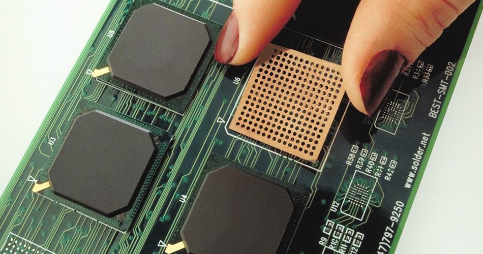
Common soldering defects and solutions in PCBA processing
PCBA processing (Printed Circuit Board Assembly) is an important part of electronic product manufacturing, and the quality of soldering directly affects the reliability and performance of the product. Common defects in the soldering process include solder joint cracking, bridging, and cold soldering. This article will explore the causes of common soldering defects in PCBA processing and provide corresponding solutions.
1. Solder joint cracking
1. Cause analysis
Solder joint cracking refers to the cracking of the solder joint in the soldering part after cooling, which is usually caused by the following reasons:
Severe temperature changes: The temperature changes too quickly during the soldering process, resulting in concentrated thermal stress in the solder joint, and cracks after cooling.
Improper selection of solder: The solder used is not strong enough to withstand the shrinkage stress after the solder joint cools down.
Substrate material problem: The thermal expansion coefficient of the substrate material and the solder is too different, resulting in solder joint cracking.
2. Solution
For the problem of solder joint cracking, the following solutions can be taken:
Control soldering temperature: Use a reasonable soldering temperature curve to avoid too fast temperature changes and reduce the thermal stress of the solder joint.
Choose the right solder: Use high-strength solder that matches the thermal expansion coefficient of the substrate material to increase the crack resistance of the solder joint.
Optimize the substrate material: Select a substrate material with a thermal expansion coefficient that matches the solder to reduce the thermal stress of the solder joint.
2. Solder bridging
1. Cause analysis
Solder bridging refers to the excess solder between adjacent solder joints, forming a bridge short circuit, which is usually caused by the following reasons:
Too much solder: Too much solder is used during the soldering process, resulting in excess solder forming a bridge between adjacent solder joints.
Too high soldering temperature: Too high soldering temperature increases the fluidity of the solder, which easily forms a bridge between adjacent solder joints.
Printing template problem: The unreasonable design of the opening of the printing template leads to excessive solder deposition.
2. Solution
For the problem of solder bridging, the following solutions can be taken:
Control the amount of solder: Reasonably control the amount of solder used to ensure that the amount of solder for each solder joint is appropriate to avoid excess solder forming a bridge.
Adjust the soldering temperature: Use appropriate soldering temperature to reduce the fluidity of solder and prevent bridge formation.
Optimize the printing template: Design reasonable printing template openings to ensure uniform solder deposition and reduce excess solder.
III. Cold solder joints
1. Cause analysis
Cold solder joints refer to solder joints that appear to be good but are actually in poor contact, resulting in unstable electrical performance. This is usually caused by the following reasons:
The solder is not fully melted: The soldering temperature is insufficient, resulting in incomplete melting of the solder and poor contact with the pad and component pins.
Insufficient soldering time: The soldering time is too short, and the solder fails to fully infiltrate the pad and component pins, resulting in cold solder joints.
Presence of oxides: Oxides exist on the surface of the pad and component pins, affecting the wetting and contact of the solder.
2. Solution
For the problem of cold solder joints, the following solutions can be taken:
Increase the soldering temperature: Ensure that the soldering temperature is high enough to fully melt the solder and increase the contact area of the solder joint.
Extend the soldering time: Prolong the soldering time appropriately to allow the solder to fully infiltrate the pads and component pins to ensure good contact.
Clean the soldering surface: Clean the oxides on the surface of the pads and component pins before soldering to ensure that the solder can fully infiltrate and contact.
IV. Solder joint pores
1. Cause analysis
Solder joint pores refer to bubbles inside or on the surface of the solder joints, which are usually caused by the following reasons:
Impurities in the solder: The solder contains impurities or gases, which form pores during the soldering process.
High humidity in the soldering environment: The humidity in the soldering environment is high, the solder is damp, and gas is generated during the soldering process, forming pores.
The pad is not fully cleaned: There are impurities or contaminants on the surface of the pad, which affect the fluidity of the solder and form pores.
2. Solution
For the problem of solder joint pores, the following solutions can be taken:
Use high-purity solder: Choose high-purity, low-impurity solder to reduce the formation of pores.
Control the humidity of the soldering environment: Maintain appropriate humidity in the soldering environment to prevent the solder from getting damp and reduce the formation of pores.
Clean the pad: Fully clean the impurities and contaminants on the surface of the pad before soldering to ensure the fluidity and good contact of the solder.
Conclusion
In PCBA processing, common soldering defects such as solder joint cracking, solder bridging, cold solder joints and solder joint pores will affect the quality and reliability of the product. By understanding the causes of these defects and taking corresponding solutions, the soldering quality of PCBA processing can be effectively improved to ensure the stability and safety of the product. With the continuous advancement of technology and the optimization of processes, the soldering quality of PCBA processing will be further improved, providing a solid guarantee for the reliability and performance of electronic products.
Send Inquiry
-
Delivery Service


-
Payment Options


