
- English
- Español
- Português
- русский
- Français
- 日本語
- Deutsch
- tiếng Việt
- Italiano
- Nederlands
- ภาษาไทย
- Polski
- 한국어
- Svenska
- magyar
- Malay
- বাংলা ভাষার
- Dansk
- Suomi
- हिन्दी
- Pilipino
- Türkçe
- Gaeilge
- العربية
- Indonesia
- Norsk
- تمل
- český
- ελληνικά
- український
- Javanese
- فارسی
- தமிழ்
- తెలుగు
- नेपाली
- Burmese
- български
- ລາວ
- Latine
- Қазақша
- Euskal
- Azərbaycan
- Slovenský jazyk
- Македонски
- Lietuvos
- Eesti Keel
- Română
- Slovenski
- मराठी
- Srpski језик

Device packaging and size standards in PCBA processing
In PCBA processing, device packaging and size standards are very important factors, which directly affect the design, manufacturing and performance of circuit boards. Here is key information about both areas:
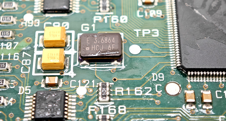
1. Device Packaging:
Device packaging refers to the external packaging or housing of electronic components (such as integrated circuits, capacitors, resistors, etc.), which provide protection, connection, and heat dissipation. Different types of device packaging are suitable for different applications and environmental requirements for PCBA. Here are some common device packaging types:
Surface Mount Package (SMD): SMD device packages are typically used in Surface Mount Technology (SMT) where components are directly attached to the PCB. Common SMD packaging types include QFN, QFP, SOP, SOT, etc. They are typically small, lightweight and suitable for high-density designs.
Plug-in packages: These packages are suitable for components connected to the PCB through sockets or solder pins, such as DIP (dual in-line package) and TO (metal package). They are suitable for components that require frequent replacement or repair.
BGA (Ball Grid Array) Packages: BGA packages have ball array connections and are suitable for high-performance applications and high-density layouts because they provide more connection points.
Plastic and metal packages: These packages are suitable for different applications, depending on the component's thermal dissipation, EMI (electromagnetic interference) requirements and environmental conditions.
Custom packaging: Certain applications may require custom device packaging to meet special requirements.
When selecting a device package, consider the PCBA board application, thermal needs, size constraints, and performance requirements.
2. Size Standards:
PCBA dimensional standards generally follow the guidelines of the International Electrotechnical Commission (IEC) and other relevant standards organizations to ensure consistency and interoperability in the design, manufacturing and assembly of circuit boards. Here are some common sizing standards and considerations:
Board Size: Typically, circuit board dimensions are expressed in millimeters (mm) and usually conform to standard sizes such as Eurocard (100mm x 160mm) or other common sizes. But custom projects may require non-standard size boards.
Number of board layers: The number of layers of the circuit board is also an important size consideration, usually represented by 2 layers, 4 layers, 6 layers, etc. Circuit boards with different layers are suitable for different design and connection needs.
Hole diameter and spacing: Hole diameter, spacing, and hole spacing on a circuit board are also important dimensional standards that affect the mounting and connection of components.
Form Factor: The board's form factor determines the mechanical enclosure or rack it fits into, and therefore needs to be coordinated with other system components.
Pad size: The size and spacing of pads affects the soldering and connection of components, so standard specifications need to be followed.
In addition, different industries and applications may have specific dimensional standard requirements, such as military, aerospace, and medical equipment. In PCBA projects, it is important to ensure that applicable dimensional standards are followed to ensure interoperability and manufacturability of the design.
In summary, proper selection of device packaging and following appropriate sizing standards are critical to a successful PCBA project. This helps ensure board performance, reliability and interoperability while also helping to reduce design and manufacturing risks.
Send Inquiry
-
Delivery Service


-
Payment Options


