
- English
- Español
- Português
- русский
- Français
- 日本語
- Deutsch
- tiếng Việt
- Italiano
- Nederlands
- ภาษาไทย
- Polski
- 한국어
- Svenska
- magyar
- Malay
- বাংলা ভাষার
- Dansk
- Suomi
- हिन्दी
- Pilipino
- Türkçe
- Gaeilge
- العربية
- Indonesia
- Norsk
- تمل
- český
- ελληνικά
- український
- Javanese
- فارسی
- தமிழ்
- తెలుగు
- नेपाली
- Burmese
- български
- ລາວ
- Latine
- Қазақша
- Euskal
- Azərbaycan
- Slovenský jazyk
- Македонски
- Lietuvos
- Eesti Keel
- Română
- Slovenski
- मराठी
- Srpski језик

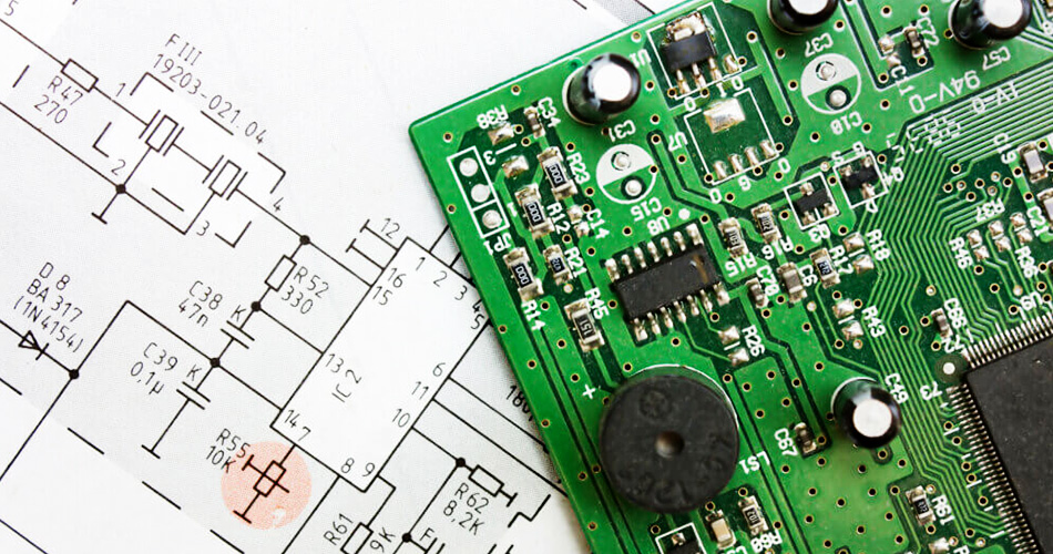
Product design optimization in PCBA processing
PCBA processing (Printed Circuit Board Assembly) is a key step in the manufacturing of electronic products, and product design optimization plays a vital role in this process. Through reasonable design optimization, not only can product performance and reliability be improved, but also production costs and production cycles can be reduced. This article will discuss in detail the product design optimization strategies and methods in PCBA processing.
1. The importance of product design optimization
In the PCBA processing process, product design optimization has the following important functions:
1. Improve product performance: By optimizing circuit design and component layout, the performance and stability of the circuit board can be improved.
2. Reduce production costs: Reasonable design optimization can reduce material waste and processing difficulty, thereby reducing production costs.
3. Shorten the production cycle: By optimizing the design, the production process can be simplified, the production cycle can be shortened, and production efficiency can be improved.
4. Improve product reliability: Optimized design can improve the product's anti-interference ability and durability, and improve product reliability.
2. Product design optimization strategy in PCBA processing
1. Reasonable component layout
Component layout is an important part of PCBA processing. Reasonable layout can improve the performance and manufacturability of the circuit board:
Reduce electromagnetic interference: separate sensitive components from interference sources to reduce electromagnetic interference.
Optimize thermal management: disperse the heat-generating components to avoid local overheating and improve heat dissipation efficiency.
Shorten the signal path: shorten the signal transmission path as much as possible to reduce signal delay and loss.
2. Fine circuit design
Fine circuit design is the key to ensuring the performance and reliability of the circuit board:
Choose appropriate trace width and spacing: According to current and voltage requirements, choose appropriate trace width and spacing to ensure circuit stability.
Avoid sharp corners and sharp turns: Avoid sharp corners and sharp turns when routing to reduce signal reflection and interference.
Increase power and ground layers: Increase power and ground layers to improve the anti-interference ability and power stability of the circuit board.
3. Use design rule checking (DRC)
Design rule checking (DRC) is an important means to ensure that the design meets manufacturing requirements:
Automatically detect design problems: Use DRC tools to automatically detect rule violations in the design to ensure that the design meets the manufacturing process requirements.
Optimize design specifications: Optimize design specifications based on DRC results to improve design quality and manufacturability.
4. Apply design simulation tools
Design simulation tools can predict and optimize the performance of circuit boards during the design stage:
Circuit simulation: Use circuit simulation tools to simulate and analyze circuit performance and optimize design parameters.
Thermal simulation: Use thermal simulation tools to simulate the thermal distribution of circuit boards, optimize component layout and heat dissipation design.
Mechanical simulation: Use mechanical simulation tools to simulate the mechanical strength and stress distribution of circuit boards and optimize structural design.
III. Actual cases of product design optimization
Case 1: Smartphone circuit board design optimization
In the design of smartphone circuit boards, electromagnetic interference and signal delay are reduced by optimizing component layout and routing design, and circuit board performance and reliability are improved. At the same time, design rule checking and design simulation tools are used to ensure that the design meets manufacturing process requirements.
Case 2: Design optimization of automotive electronic controllers
In the design of automotive electronic controllers, the anti-interference ability and durability of circuit boards are improved by optimizing thermal management and power supply design. At the same time, circuit simulation and thermal simulation tools are used to optimize design parameters and layout to improve product reliability and performance.
IV. Challenges and solutions for product design optimization
Although product design optimization has many advantages in PCBA processing, it also faces some challenges in practical applications:
Complex design requirements: With the increase in the functions of electronic products, design requirements are becoming more and more complex. The solution is to improve design efficiency and quality by introducing advanced design tools and methods.
Shortage of technical talents: High-level design optimization requires technical talents with rich experience and professional knowledge. The solution is to strengthen technical training and talent introduction to improve the overall level of the design team.
Cost control pressure: While optimizing the design, enterprises are facing the pressure of cost control. The solution is to reduce design and production costs by optimizing the design process and improving production efficiency.
Conclusion
In PCBA processing, through reasonable product design optimization, enterprises can significantly improve product performance and reliability, reduce production costs and shorten production cycles. Through reasonable component layout, sophisticated circuit design, design rule checking and design simulation tools, enterprises can achieve high-quality design optimization and meet the market demand for high-performance and high-reliability electronic products. Although there are some challenges in practical applications, these challenges can be overcome through reasonable planning and continuous improvement. PCBA processing companies should actively adopt advanced design optimization strategies and methods to enhance product competitiveness and lay a solid foundation for future development.
Send Inquiry
-
Delivery Service


-
Payment Options


