
- English
- Español
- Português
- русский
- Français
- 日本語
- Deutsch
- tiếng Việt
- Italiano
- Nederlands
- ภาษาไทย
- Polski
- 한국어
- Svenska
- magyar
- Malay
- বাংলা ভাষার
- Dansk
- Suomi
- हिन्दी
- Pilipino
- Türkçe
- Gaeilge
- العربية
- Indonesia
- Norsk
- تمل
- český
- ελληνικά
- український
- Javanese
- فارسی
- தமிழ்
- తెలుగు
- नेपाली
- Burmese
- български
- ລາວ
- Latine
- Қазақша
- Euskal
- Azərbaycan
- Slovenský jazyk
- Македонски
- Lietuvos
- Eesti Keel
- Română
- Slovenski
- मराठी
- Srpski језик

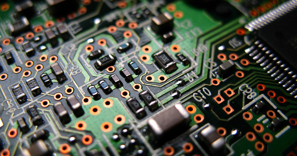
Electromagnetic compatibility design in PCBA processing
Electromagnetic compatibility design (EMC) refers to the use of scientific and reasonable design and process means to ensure that electronic equipment can operate normally in its working environment, and is not subject to electromagnetic interference from other electronic equipment, nor does it interfere with other equipment. In the PCBA process, electromagnetic compatibility design is particularly important because it directly affects the stability and reliability of the product.
1. Sources of electromagnetic interference
In the PCBA process, there are two main sources of electromagnetic interference (EMI): internal interference and external interference.
Internal interference:
Internal interference refers to the electromagnetic interference generated between components on the circuit board. For example, high-frequency signal lines may interfere with adjacent low-frequency signal lines, and switching power supplies may also interfere with surrounding circuits. In order to reduce internal interference, electromagnetic compatibility needs to be fully considered in circuit design and component layout.
External interference:
External interference refers to electromagnetic interference from the external environment, such as wireless signals, electromagnetic radiation from surrounding equipment, etc. External interference may affect the normal operation of the circuit board through power lines, signal lines or direct radiation. In response to external interference, shielding and filtering measures need to be taken to improve the anti-interference ability of the circuit board.
2. Electromagnetic compatibility design strategy in PCBA processing
Reasonable layout:
Reasonable component layout is the basis for achieving electromagnetic compatibility design. During PCBA processing, engineers need to separate noise-sensitive components from noise sources according to circuit functions and working characteristics. For example, high-frequency circuits and low-frequency circuits should be separated as much as possible, and high-speed signal lines should be as short and straight as possible to avoid crossing with other signal lines.
Design of power supply and ground:
The design of power supply and ground wire has a great impact on electromagnetic compatibility. In PCBA processing, multi-layer board design should be used as much as possible to provide independent power supply layer and ground layer to reduce the impedance of power supply and ground wire. In addition, decoupling capacitors should be added between power supply and ground wire to suppress the propagation of high-frequency noise.
Signal integrity:
Signal integrity refers to the signal maintaining its original waveform and amplitude during transmission. In PCBA processing, ensuring signal integrity is an important part of achieving electromagnetic compatibility design. To this end, it is necessary to perform terminal matching on high-speed signal lines to avoid reflection interference; differential routing on key signal lines to reduce electromagnetic radiation.
Shielding and filtering:
Shielding and filtering are important means to prevent external electromagnetic interference. In PCBA processing, external electromagnetic interference can be blocked by adding metal shielding covers or shielding layers at key locations. In addition, filters can be added to power lines and signal lines to filter out high-frequency interference signals and improve the anti-interference ability of circuit boards.
3. Necessity of electromagnetic compatibility testing
After PCBA processing is completed, electromagnetic compatibility testing is an important step to ensure that the product meets relevant standards and requirements. Electromagnetic compatibility testing includes radiated emission testing, conducted emission testing, radiated immunity testing, and conducted immunity testing, etc., to comprehensively evaluate the electromagnetic compatibility performance of circuit boards.
4. Commonly used test methods
Common electromagnetic compatibility test methods include near-field scanning, far-field measurement, and electromagnetic shielding effectiveness testing. Through these tests, problems in electromagnetic compatibility design can be discovered in a timely manner, and corresponding adjustments and improvements can be made to ensure the electromagnetic compatibility of products.
Conclusion
In the process of PCBA processing, electromagnetic compatibility design is a key link to improve product performance and reliability. The electromagnetic compatibility performance of the circuit board can be effectively improved by reasonable layout, optimizing power and ground line design, ensuring signal integrity, and taking shielding and filtering measures. Through advanced electromagnetic compatibility testing, problems can be discovered and improved in a timely manner to ensure that the product meets relevant standards and requirements. Electromagnetic compatibility design can not only improve product quality and reliability, but also enhance product competitiveness in the market.
Send Inquiry
-
Delivery Service


-
Payment Options


