
- English
- Español
- Português
- русский
- Français
- 日本語
- Deutsch
- tiếng Việt
- Italiano
- Nederlands
- ภาษาไทย
- Polski
- 한국어
- Svenska
- magyar
- Malay
- বাংলা ভাষার
- Dansk
- Suomi
- हिन्दी
- Pilipino
- Türkçe
- Gaeilge
- العربية
- Indonesia
- Norsk
- تمل
- český
- ελληνικά
- український
- Javanese
- فارسی
- தமிழ்
- తెలుగు
- नेपाली
- Burmese
- български
- ລາວ
- Latine
- Қазақша
- Euskal
- Azərbaycan
- Slovenský jazyk
- Македонски
- Lietuvos
- Eesti Keel
- Română
- Slovenski
- मराठी
- Srpski језик

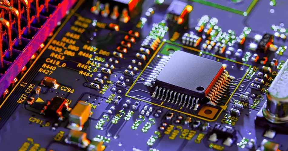
Anti-interference design in PCBA processing
In PCBA (Printed Circuit Board Assembly) processing, anti-interference design is the key to ensure the stability and reliability of electronic products. Electromagnetic interference (EMI) and radio frequency interference (RFI) may cause abnormal function or failure of circuit boards, so it is very important to take effective anti-interference design measures during PCBA processing. This article will explore how to implement anti-interference design in PCBA processing, including reasonable layout design, selection of appropriate materials, use of shielding technology, and optimization of power supply design.
Reasonable layout design
1. Component layout optimization
Component layout optimization is the basis of anti-interference design. By reasonably arranging components on the circuit board, interference between interference sources and sensitive areas can be reduced.
Separate sensitive circuits: Arrange high-frequency signal lines and low-frequency signal lines separately to reduce interference between signals.
Reasonable wiring: Avoid long cables and cross wiring, shorten signal paths, and reduce the possibility of signal attenuation and interference.
Add ground wires: Arrange enough ground wires on the circuit board to provide a stable ground reference and reduce the impact of interference on the circuit.
Implementation strategy: Conduct detailed circuit layout analysis in the design stage to ensure the rationality of components and wiring and reduce interference risks.
Choose the right material
1. Use anti-interference materials
Choosing the right material is crucial to improving the anti-interference ability of the circuit board. Anti-interference materials can effectively reduce electromagnetic interference and radio frequency interference.
High-frequency PCB substrate: Select a PCB substrate with good high-frequency performance, such as PTFE or ceramic substrate, to reduce signal loss and interference.
Anti-interference coating: Use anti-interference coating or shielding material to cover the sensitive areas of the circuit board to prevent external interference.
Implementation strategy: According to the operating frequency and environmental requirements of the circuit board, select appropriate materials and coatings to improve the anti-interference performance of the circuit board.
Use shielding technology
1. Electromagnetic shielding
Electromagnetic shielding technology reduces the impact of interference on the circuit by physically isolating interference sources and sensitive areas.
Metal shielding cover: Use a metal shielding cover to cover the key areas of the circuit board to prevent electromagnetic waves from entering or leaving these areas.
Shielding frame: Set a shielding frame outside the circuit board to protect the circuit board from external interference.
Implementation strategy: Consider the application of electromagnetic shielding technology in the design, select appropriate shielding materials and structures, and ensure the anti-interference ability of the circuit board.
2. Grounding technology
Good grounding technology can effectively reduce interference and noise and provide a stable ground reference.
Ground plane: Use the ground plane as the ground reference of the circuit board to reduce ground impedance and interference.
Grounding holes: Arrange enough grounding holes on the circuit board to ensure good conduction and stability of the current.
Implementation strategy: Optimize the grounding design to ensure the stability of the ground reference of the circuit board and improve the anti-interference performance.
Optimize power supply design
1. Power supply filtering
Power supply filtering can effectively reduce power supply noise and interference and improve the stability of the circuit board.
Filter: Add filters such as LC filters or RC filters to the power supply line to filter out high-frequency noise and interference.
Decoupling capacitor: Add decoupling capacitors near the power pins to reduce the impact of power supply noise on the circuit.
Implementation strategy: Select appropriate filters and decoupling capacitors, optimize the design according to the power supply noise characteristics, and improve the stability and anti-interference ability of the power supply.
2. Power supply layout
Power supply layout optimization helps reduce power supply interference and noise.
Power line layout: Lay the power line and signal line separately to reduce the interference of power supply noise on the signal.
Power layer design: Use a dedicated power layer in a multi-layer PCB to provide a stable power supply and reduce noise.
Implementation strategy: Optimize the design of power lines and power layers to ensure stable power supply and reduce the impact of power noise on the circuit.
Summary
In PCBA processing, anti-interference design is the key to improving the stability and reliability of electronic products. Through reasonable layout design, selection of appropriate materials, use of shielding technology and optimization of power supply design, electromagnetic interference and radio frequency interference can be effectively reduced, and the anti-interference ability of the circuit board can be improved. The implementation of these measures will help improve the performance and reliability of the product, thereby enhancing the market competitiveness of the enterprise.
Send Inquiry
-
Delivery Service


-
Payment Options


