
- English
- Español
- Português
- русский
- Français
- 日本語
- Deutsch
- tiếng Việt
- Italiano
- Nederlands
- ภาษาไทย
- Polski
- 한국어
- Svenska
- magyar
- Malay
- বাংলা ভাষার
- Dansk
- Suomi
- हिन्दी
- Pilipino
- Türkçe
- Gaeilge
- العربية
- Indonesia
- Norsk
- تمل
- český
- ελληνικά
- український
- Javanese
- فارسی
- தமிழ்
- తెలుగు
- नेपाली
- Burmese
- български
- ລາວ
- Latine
- Қазақша
- Euskal
- Azərbaycan
- Slovenský jazyk
- Македонски
- Lietuvos
- Eesti Keel
- Română
- Slovenski
- मराठी
- Srpski језик


Neck Massager PCBA
Since 2008, Unixplore Electronics has been providing one-stop turnkey manufacture and supply services for high-quality neck massager PCBA in China. The company is certified with ISO9001:2015 and adheres to the PCB assembly standard of IPC-610E.
Send Inquiry
Product Description
How to design neck massager PCBA control board?
If you are looking for a comprehensive selection of neck massager PCBA manufactured in China, Unixplore Electronics is your ultimate source. Their products are priced very competitively and accompanied by top-notch after-sales service. Moreover, they have been actively seeking WIN-WIN collaborative relationships with customers from all over the world.
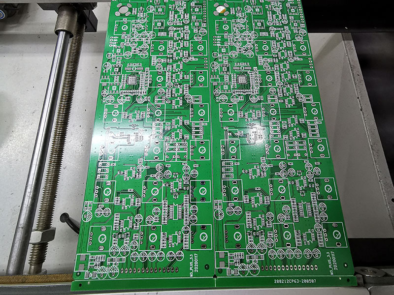
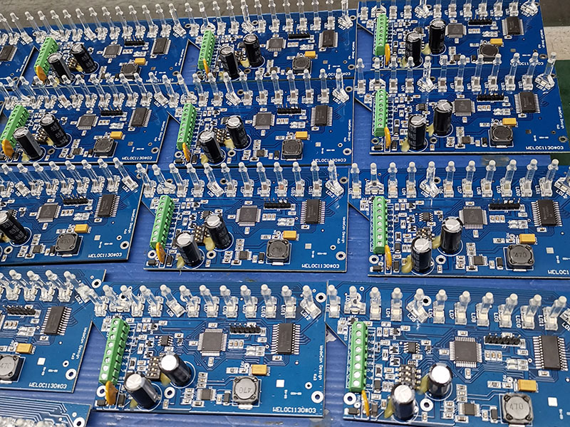
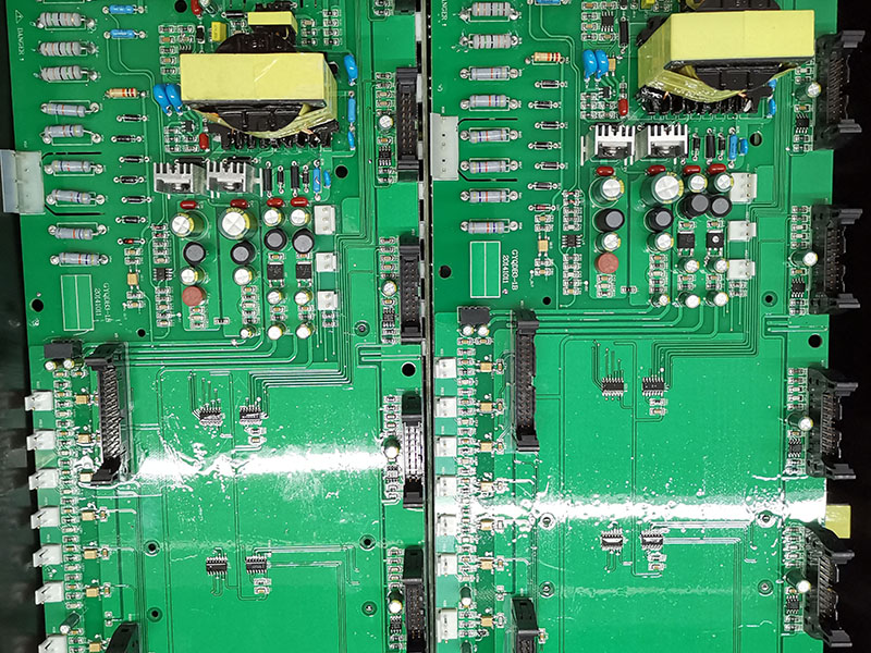
The neck massager PCBA(Printed Circuit Board Assembly) is the core part of the neck massage instrument. It usually includes power circuits, control circuits, massage circuits, and display circuits.The power supply circuit mainly provides electrical energy for the neck massager, and has protection functions, such as overcurrent protection and overvoltage protection.
Control circuit is responsible for the control of the entire neck massage instrument, including massage time, massage mode and massage strength.
The massage circuit is the core part of the neck massage instrument. It outputs the massage energy according to the instructions of the control circuit to achieve the massage effect. Different neck massage instruments have different massage circuits, such as pulse, kneading, and knocking.
The display circuit indicates massage information and parameters, which is convenient for patients to view and understand.
When designing the neck massager PCB, the following aspects need to be considered:
Safety and reliability: The neck massage instrument is a device used for treatment. Therefore, the design of the circuit board needs to ensure safety and reliability and avoid accidents.
Accuracy and stability: The neck massage instrument needs to accurately output massage energy, so the design of the circuit board needs to ensure accuracy and stability to ensure the treatment effect.
Easy to produce and maintain: The design of the neck massage instrument board needs to be considered as easy to produce and maintain, such as the selection of device, the layout and structure of the circuit board, which will directly affect production efficiency and maintenance costs.
Appearance design: The design of the neck massage instrument board also needs to consider the design, including the size, shape, color, etc. of the circuit board to meet the needs of users and aesthetics.
Unixplore provides one-stop turnkey service for your EMS project. Feel free to contact us for your board building, we can make a quotation in 24 hours after we receive your Gerber file and BOM list!
Neck Massager PCBA manufacture
* Gerber file and BOM list supplied by client
* Blank PCB made, components purchased by us
* PCB fabrication with parts fully assembled
* 100% Function Tested OK before shipping
* RoHS compliant, Lead-free manufacturing process
* Quick delivery, with independent ESD package
* One stop electronic manufacturing service for PCB design, PCB layout, PCB manufacture, components procurement, PCB SMT and DIP assembly, IC programming, function test, packaging and delivery
Unixplore PCB & PCB Assembly Capability
| Parameter | Capability |
| Layers | 1-40 layers |
| Assembly Type | Through-Hole (THT), Surface Mount (SMT), Mixed (THT+SMT) |
| Minimum Component Size | 0201(01005 Metric) |
| Maximum Component Size | 2.0 in x 2.0 in x 0.4 in (50 mm x 50 mm x 10 mm) |
| Component Package Types | BGA, FBGA, QFN, QFP, VQFN, SOIC, SOP, SSOP, TSSOP, PLCC, DIP, SIP, etc. |
| Minimum Pad Pitch | 0.5 mm (20 mil) for QFP, QFN, 0.8 mm (32 mil) for BGA |
| Minimum Trace Width | 0.10 mm (4 mil) |
| Minimum Trace Clearance | 0.10 mm (4 mil) |
| Minimum Drill Size | 0.15 mm (6 mil) |
| Maximum Board Size | 18 in x 24 in (457 mm x 610 mm) |
| Board Thickness | 0.0078 in (0.2 mm) to 0.236 in (6 mm) |
| Board Material | CEM-3,FR-2,FR-4, High-Tg, HDI, Aluminum, High Frequency, FPC, Rigid-Flex, Rogers, etc. |
| Surface Finish | OSP, HASL, Flash Gold, ENIG, Gold Finger, etc. |
| Solder Paste Type | Leaded or Lead-Free |
| Copper Thickness | 0.5OZ – 5 OZ |
| Assembly Process | Reflow Soldering, Wave Soldering, Manual Soldering |
| Inspection Methods | Automated Optical Inspection (AOI), X-ray, Visual Inspection |
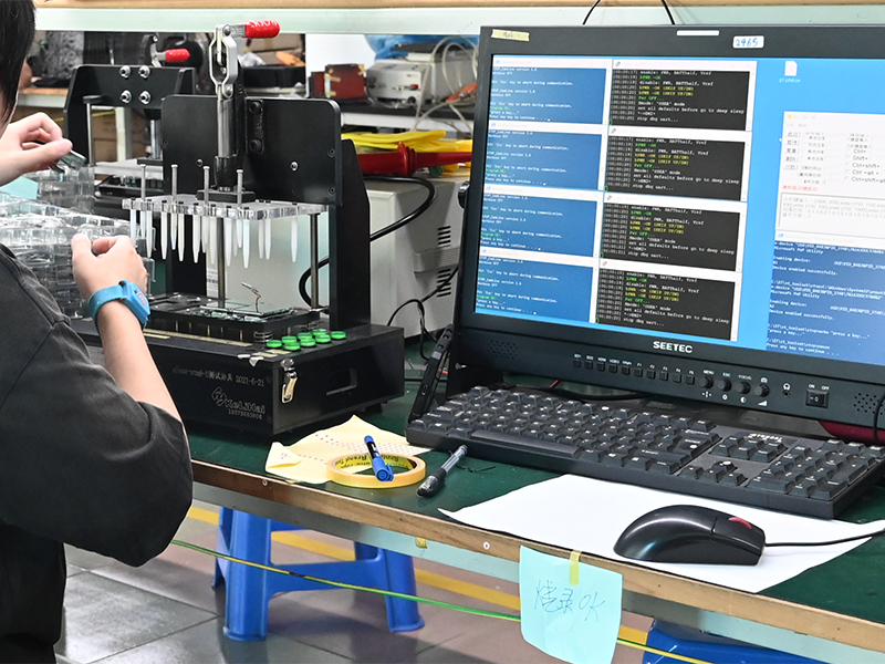
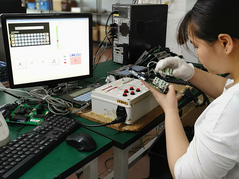
| Testing Methods In-House | Functional Test, Probe Test, Aging Test, High and Low Temperature Test |
| Turnaround Time | Sampling: 24 hours to 7 days, Mass Run: 10 - 30 days |
| PCB Assembly Standards | ISO9001:2015; ROHS, UL 94V0, IPC-610E class ll |
Unixplore Value-Added EMS Service
● IC pre-programming service with file in format of HEX,ELF and BIN.
● Neck Massager PCBA Function test fixture customized according to client’s test requirements
● Box building service including plastic & metal case mold and part production
● Conformal coating including selective lacquer coating, epoxy resin potting
● Wire harness and cable assembly
● Finished product assembly including box, screen, membrane switch, labelling and customized carton or retail box packing.
● Various third-party tests for PCBA are available upon request
● Product Certification Assistance
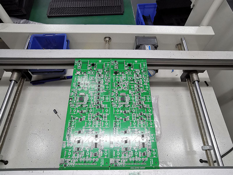
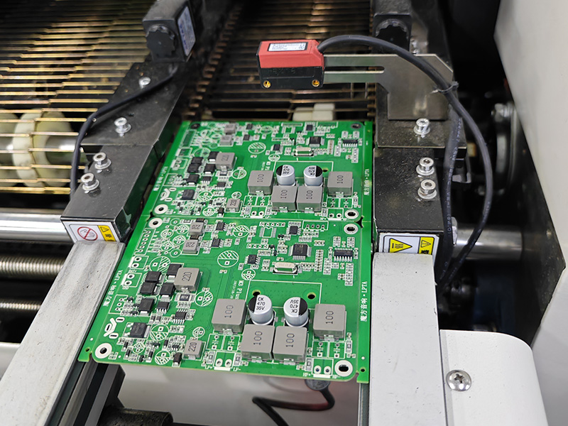
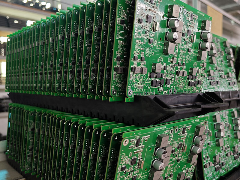
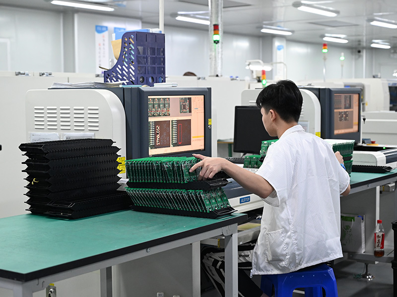
PCBA Production Procedure
-
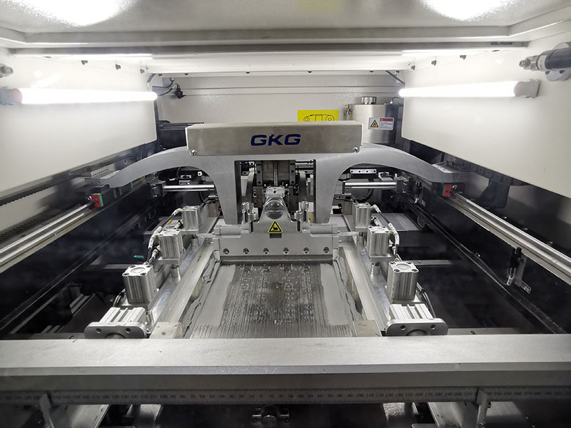
1. Automatic solderpaste printing
-
2. solderpaste printing done
-
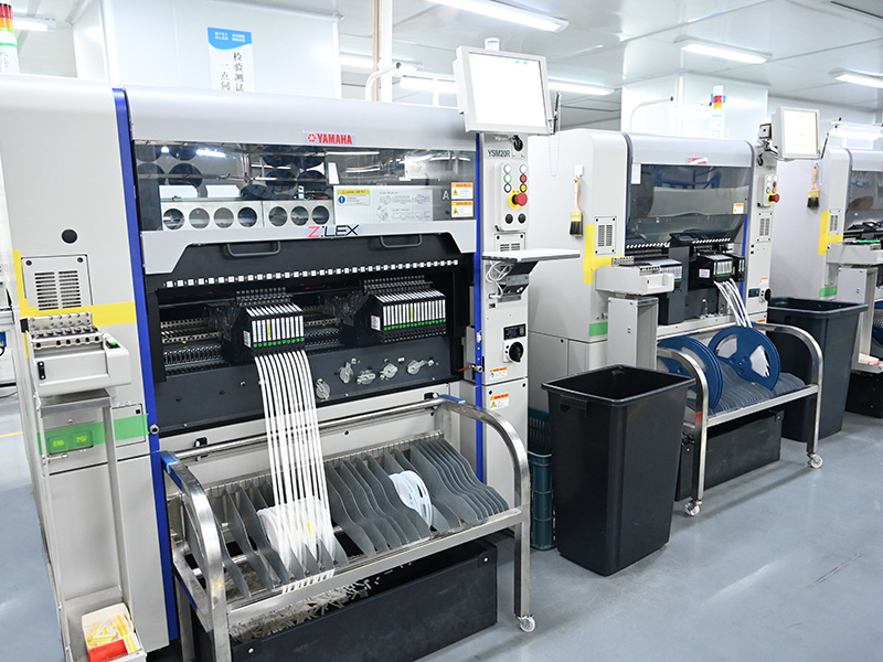
3. SMT pick and place
-
4. SMT pick and place done
-
5. ready for reflow soldering
-
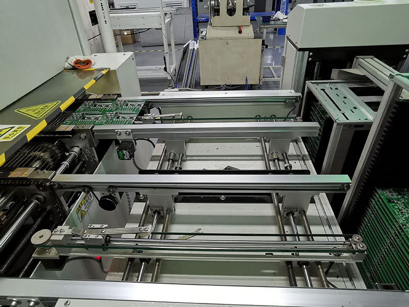
6. reflow soldering done
-
7. ready for AOI
-
8. AOI inspection process
-
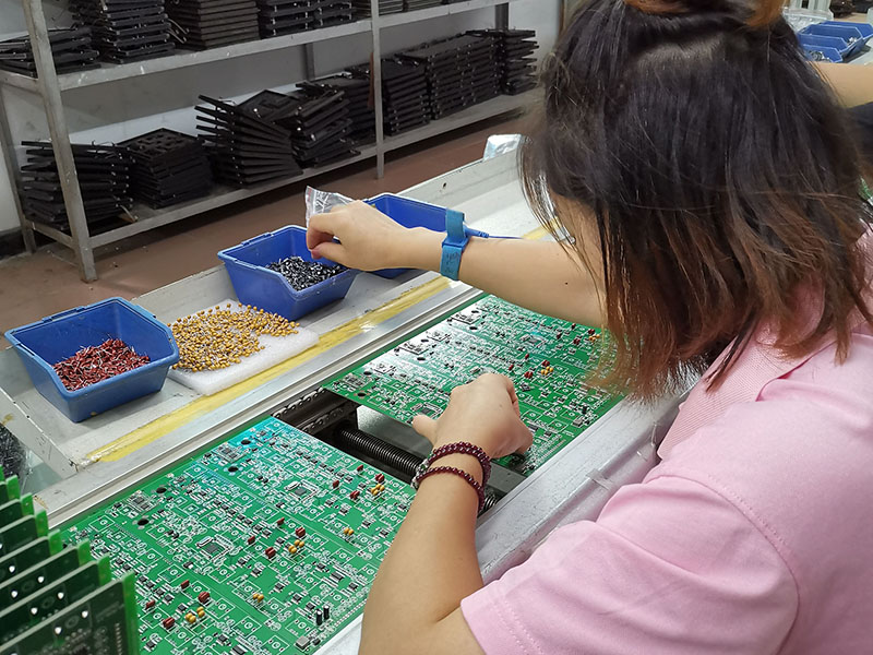
9. THT component placement
-
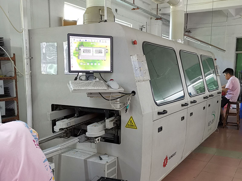
10. wave soldering process
-
11. THT assembly done
-
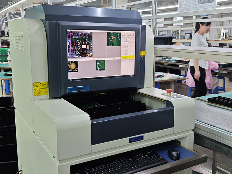
12. AOI Inspection for THT assembly
-
13. IC programming
-
14. function test
-
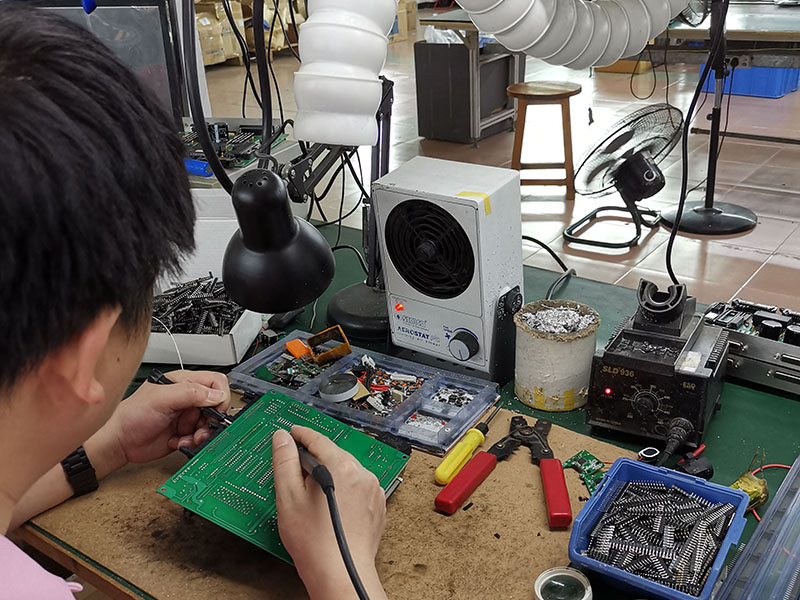
15. QC Check and Repair
-
16. PCBA conformal coating Process
-
17. ESD packing
-
18. Ready for Shipping
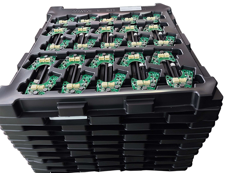
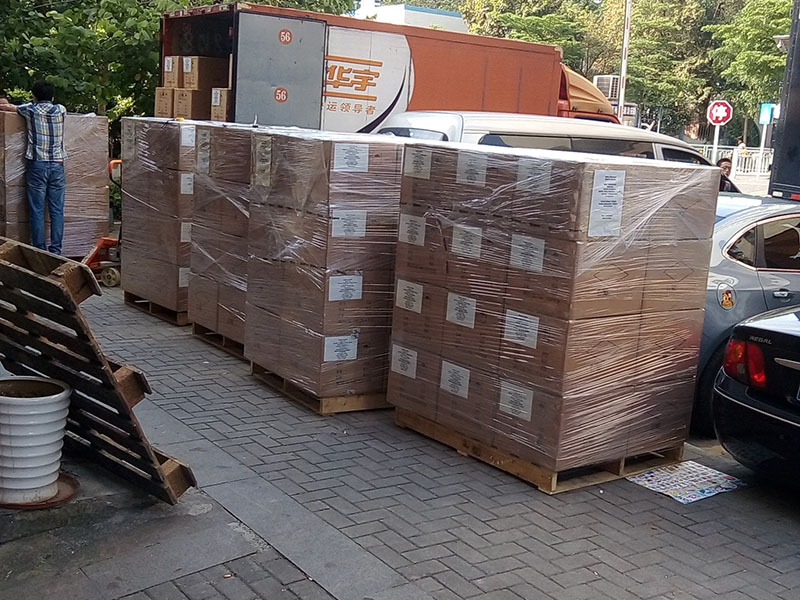
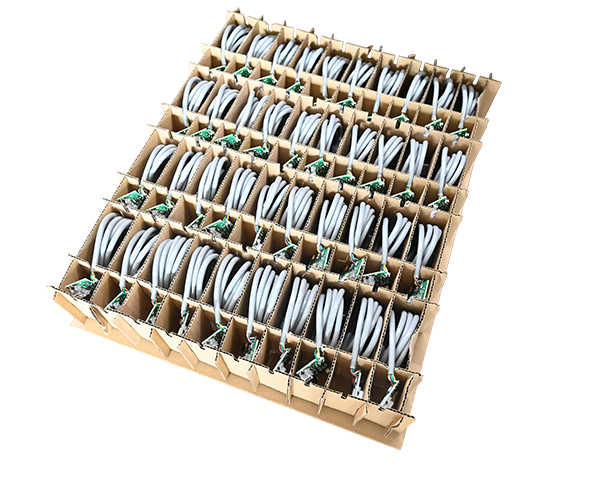
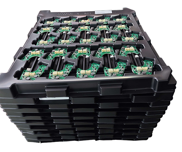
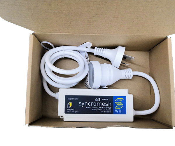
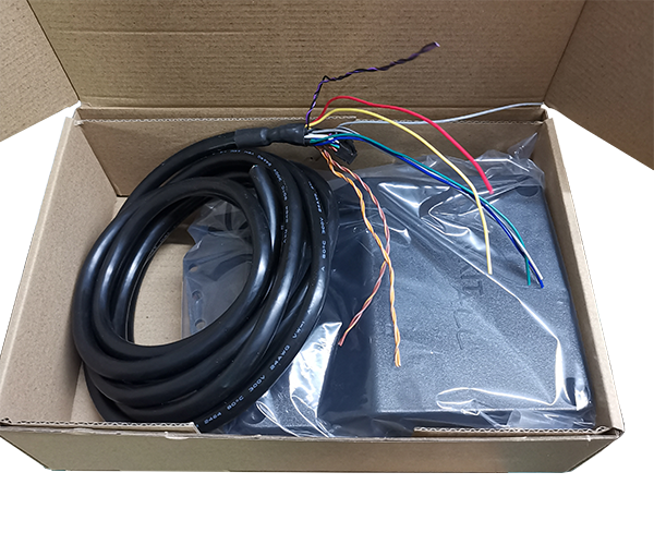
Packaging
For PCBA
For Finished Product
Hot Tags: Neck Massager PCBA, China, Manufacturers, Suppliers, Factory, Customized, Cheap, Quality, Advanced, CE, 1 Year Warranty, Price
Related Category
Home Appliance PCBA
Industrial Control PCBA
Automobile PCBA
Consumer Electronics PCBA
Medical Equipment PCBA
Security System PCBA
Healthcare PCBA
LED Lighting PCBA
IoT PCBA
Electric Gardening Tool PCBA
Send Inquiry
Please Feel free to give your inquiry in the form below. We will reply you in 24 hours.


